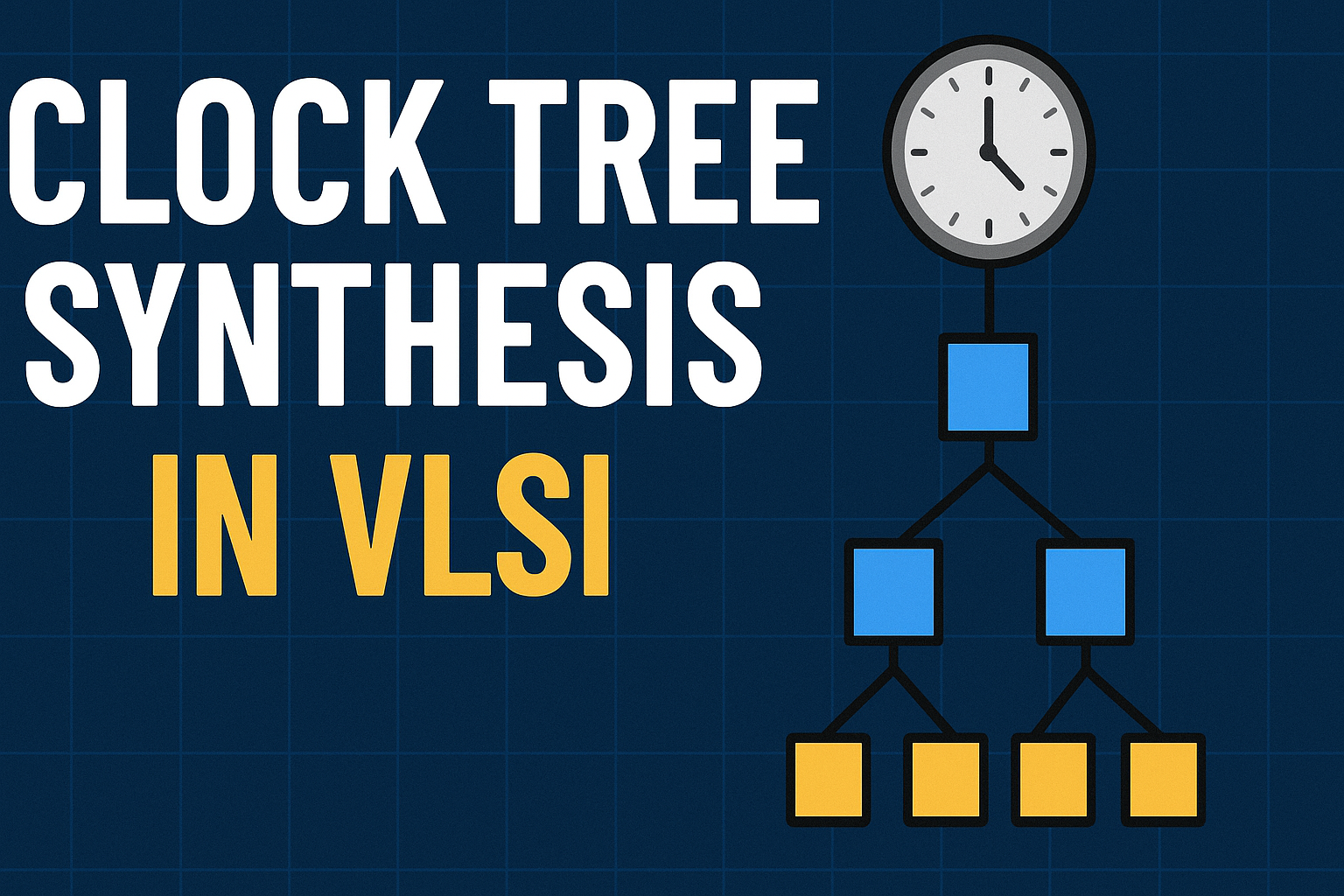
Clock Tree Synthesis (CTS) in VLSI: Skew Reduction, Latency Optimization & Clock Network Design – Part -1
Understanding Clock Tree Synthesis (CTS) in VLSI Physical Design
In the world of VLSI Physical Design, one of the most critical challenges is ensuring that all flip-flops on a chip receive the clock signal simultaneously—or as close as physically possible. This is where Clock Tree Synthesis (CTS) comes into play.
Whether you're taping out a high-performance SoC or optimizing power in a mobile chipset, timing is everything. CTS is not just a phase in the back-end design flow; it is the heartbeat of the chip, orchestrating synchronous operations across millions (sometimes billions) of transistors.
A Pizza Analogy: Demystifying CTS
Let’s break it down with a simple analogy.
Imagine a bustling city with hundreds of hungry residents waiting for their pizzas. There’s one big pizza kitchen (the clock source) that must deliver to every home (flip-flops) in town. The goal? Ensure everyone receives hot, fresh pizza at the same time.
Without Coordination:
- One delivery person tries to serve everyone in a giant loop.
- Some get cold pizza, some wait too long.
- The whole system breaks down due to inefficient routing and timing delays.
With Smart Coordination (Like CTS):
- The city is divided into zones.
- Multiple delivery agents (like clock buffers) serve localized areas.
- Delivery paths are optimized so everyone gets their pizza at the same time.
- Result: Hot, synchronized delivery—just like clock signals reaching flip-flops in sync.
What Is CTS in Technical Terms?
Clock Tree Synthesis is the process of creating a balanced and buffered distribution network that delivers the clock signal from a central source (like a PLL) to all clock sinks (flip-flops, latches) in the design.
Unlike standard signal routing, the clock network is highly sensitive—it can consume 30–60% of the chip’s dynamic power. Even minor imperfections in clock distribution can lead to setup and hold violations, impacting chip functionality.
Key Objectives of CTS
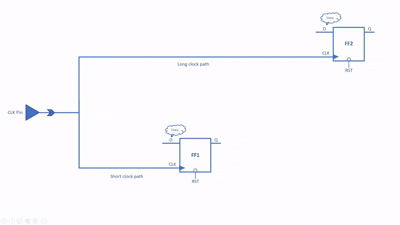
- Minimize Clock Skew: Skew is the time difference between clock signal arrivals at different flip-flops. Excess skew leads to setup/hold violations and unreliable timing behavior.
- Reduce Clock Latency: Latency is the delay from the clock source to the sinks. Lower latency improves timing margins and supports faster clock frequencies.
- Maintain Clock Balance: Balanced trees ensure that all parts of the chip operate in a synchronized manner, especially critical in multi-clock domain designs.
- Optimize for Power and Signal Integrity: Efficient buffer insertion helps manage IR drop, avoid electromigration (EM) issues, and reduce unnecessary dynamic power consumption.
How Does CTS Work? | The Workflow
- Clock Tree Definition: Tools identify all clock sources and sinks, defining the overall topology.
- Buffer Insertion: Buffers are strategically placed to drive high fanout and maintain load balance.
- Skew Optimization: Tools reshape the tree to equalize path delays, minimizing skew.
- CTS Routing: Physical metal routes for the clock tree are created based on congestion and DRC guidelines.
- Clock Gating Support: Incorporates clock gating cells to reduce dynamic power in idle modules.
- Post-CTS Analysis: Designers perform skew, latency, and power analysis to validate the clock network's performance.
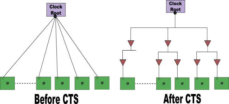
Common Clock Tree Structures
- Balanced Tree (Buffered Tree): Uniform depth and delay paths.
- H-Tree Structure: Geometric symmetry for large-scale designs.
- Clock Mesh: Robustness against variation; used in high-performance CPUs and ASICs.
CTS: Where Engineering Meets Art
Mastering Clock Tree Synthesis isn’t just about understanding tools—it’s about learning to balance performance, power, and timing integrity . It requires experience, intuition, and knowledge of EDA tools like Innovus , ICC2, etc.
A well-synthesized clock tree can make or break timing closure, especially in designs with aggressive PPA (Power, Performance, Area) targets.
 Mostak Ahmmed, Engineer-III