Cost Efficient Semiconductor Testing: From Wafer to Product
28 Aug 2025 | 05:14 PM
10 min read
In the past, more than 30% of chips failed or were discarded due to undetected defects, causing low yield (<70%) and costly delays.
Debugging was slow due to limited visibility into faults. We solve this with an end-to-end testing flow, from wafer-level probing to system-level validation.
Our modular daughter card, designed for the Advantest platform, allows easy reuse across devices.
This approach supports both analog and digital chips with fewer hardware changes delivering high-quality results while reducing cost and time-to-market.
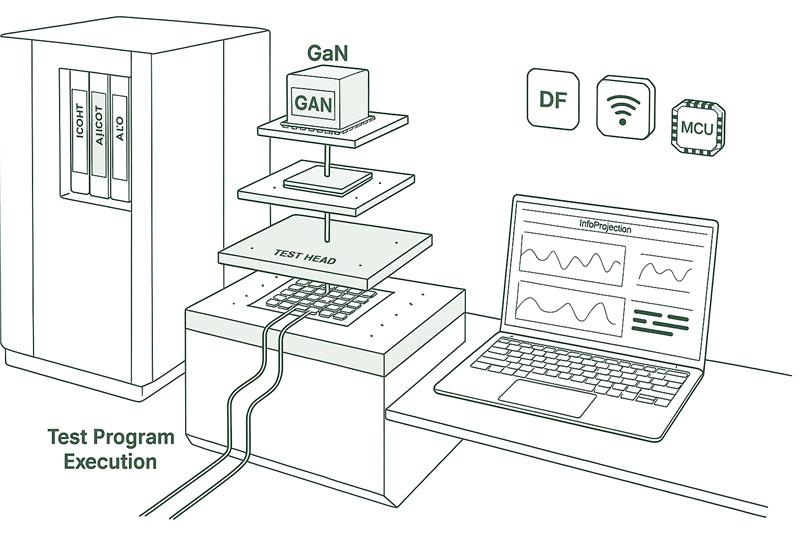
Testing Flow Overview
Why is Testing Necessary?
- Ensures correct functionality of the chip before and after fabrication.
- Detects manufacturing defects, design flaws, and aging effects.
- Enhances product quality, yield, and customer trust.
- Reduces the risk of failure in the field.
- Yield Analysis.
- Failure Diagnosis.
- Future Design Improvements.

Wafer-Level Testing:
- Uses probe cards to test each die on wafer.
- Identify bad dies early to save cost.
Package-Level Testing:
- After dicing and packaging, further functional/electrical tests are done.
How Much Time Testing Takes?
- ~30% to 50% of the total manufacturing effort can be spent on testing.
- Higher complexity → More test patterns → Longer test time.
Plug, Play and Perform: The Design that Changes the Game
- Load Board Design: Enabling safe, high-performance testing with integrated protection.
- Plug-and-Play Innovation: Test multiple devices effortlessly with seamless hardware-software integration.
- Smart Software Control: Automate and customize test programs for maximum efficiency.
- Reusable Tester Resources: Optimize channel usage for cost-effective, scalable testing.
- Safety First Approach: Built-in protection equipment ensures secure testing environments.
- Next-Level Reliability: Streamlined strategy for consistent, high-quality results.
Short Description of Tested Product on V93K ATE
GaN Devices:
- OCP, OTP, Gate protection & high voltage protection circuitries.
- Tested in different operating modes (Normal & low power mode).
- 600V generation on Board.
- Supplied pulsed current and measured on-state resistance.
ADC Devices:
- AC & DC accuracy check in different power mode
- On board signal amplification & filtration
- On board signal generation maintaining ultra-low noise
Gain Amplifier Devices:
- Multiple Test Setup On Single Implementation
- Ensuring Signal Integrity Among Multiple Components
- Compact Test Setup With Proper Placing For Multisite Testing
Microcontroller Devices:
- Power On Reset and Brown Out Reset test
- Measured high frequency using Timing Measure Unit
- Tested Electrical characteristics
Challenges and Solution
| Category | Challenges | Solutions |
|---|---|---|
| GaN | High voltage risks in GaN power systems | Integrated safety circuits in Load Board design to mitigate voltage hazards |
| Thermal management under heavy loads | Advanced cooling mechanisms and real-time monitoring via software control | |
| Device reliability during plug-and-play testing | Robust protection equipment and reusable channels for consistent performance |
| Category | Challenges | Solutions |
|---|---|---|
| RF | Multiple test setups with plug-and-play option | Made an automated software-controlled module containing multiple test setups |
| Signal integrity issues | Ensured proper signal integrity in stimuli and receiving sides by maintaining appropriate equipment | |
| Larger components | Replaced with alternative components having a smaller footprint |
| Category | Challenges | Solutions |
|---|---|---|
| ADC | Clean, pure input signal required for linearity testing | Used a 32-bit DAC and MCU for analog signal generation, with a low-pass filter to eliminate high-frequency noise |
| Stable reference voltage supply in the ADC | Used onboard precision voltage reference | |
| ADC output data processing | Employed mixed-signal and DSP-based testing methodologies for efficient data processing |
Cost efficiency: Test More, Spend Less
- Hardware reuse
- Load Board reconfigurability
- Minimum ATE test time per device
- On board designed circuitries
- Open-source tool used to design Load board.
Tomorrow’s Silicon, Today’s Strategy:
- Machine Learning Based Test Optimization: Intelligent algorithms will analyze test data trends, dynamically adapt test conditions, and predict failures—significantly reducing pattern count and test time.
- Fully Reusable Load Board Architecture: Daughter card-based modular load boards will support faster test reconfiguration and hardware reuse across product lines, reducing cost per device.
- Testing Support for Emerging Nodes: Advanced techniques will be needed to support 2nm, 3D-IC, and GaN-on-Si technologies, addressing higher power density, tighter geometries, and complex fault behaviors.
The Economic Ripple of Innovation
- Fosters Local Innovation & Employment: Generates high-skill jobs and empowers local chip and hardware startups by providing cost-effective testing solutions.
- Boosts Economic Growth: Strengthens Bangladesh’s economy by nurturing a high-value tech ecosystem.
- Conserves Foreign Currency: Minimizes reliance on expensive foreign testing platforms, retaining financial resources within the local economy.
- Attracts Investment: Encourages domestic and foreign investment in the semiconductor sector by offering affordable, scalable testing infrastructure.
- Enhances Export Potential: Enables local startups to produce high-quality, competitively priced hardware, boosting exports and global market presence.
- Drives National Self-Reliance: Aligns with Bangladesh’s vision of a self-sufficient, technology-driven future in the semiconductor industry.
 Abdullah Al Imran Ifrit, Engineer III
 Mohidul Islam Khan Robin, Engineer III
 Abdul Mumin Redhowan, Engineer I